
With so many people relying on the apps on their phones, glitches can feel like the end of the world.
Devices shielded from outside signals are less likely to experience sudden runtime problems.
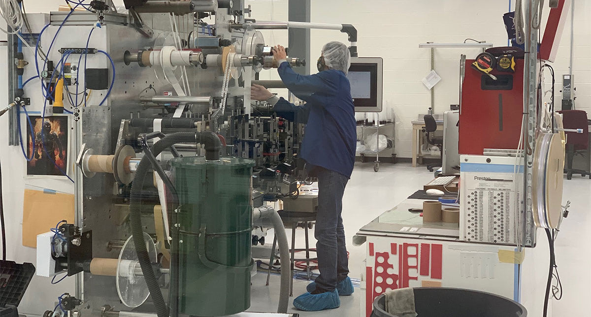
When working with sensitive technology, it’s necessary to take design precautions against signal interference. In the past, Strouse has built EMI shielding components for cars, computers, and more.
Today, you’ll learn how shielding your components from signal interference reduces the number of technology malfunctions and otherwise benefits you.
What are EMI and RFI Shielding?
Electromagnetic Interference (EMI) and Radio Frequency Interference (RFI) are caused by signals emitted from technology or weather phenomena. These signals can disturb device systems and cause problems with their functionality.
While EMI is born from short-range, high-pitched interference emitting from the devices, RFI comes from the same spectrum but refers to longer wavelengths from external sources.
What’s the Benefit of Proper EMI and RFI Shielding Techniques?
EMI and RFI can be as simple as one device preventing another electronic device from properly operating. For example, an electronic watch could inadvertently alter the volume on your TV.
In more severe cases, poorly designed consumer electronics that forgo RFI and EMI shielding can even endanger users or bystanders.
Proper EMI and RFI shielding is crucial for many applications. Today, you’ll see the benefits so you can plan and execute the perfect design.
1. AVOIDING MACHINE FAILURE
The effects of radio frequency interference and electromagnetic interference can cause unpredictable and non-repeatable degradation of instrument performance and accuracy, and even cause complete instrument failure.
Complete instrument failure can result in reduced production efficiency, increased return dollars, plant shutdowns, and sometimes dangerous safety hazards.
Putting in the work by testing samples or taking other precautions during product development will ensure the product meets proper EMI shielding standards.
2. IMPROVING SHIELDING CAPABILITIES
It can be challenging to alter a pre-existing design, mainly when the number of layers in a device is already limited, with tight margins. However, bolstering the shielding capabilities of a design might be critical for reducing performance issues.
Improving a device’s resistance towards EMI could eliminate signal errors and improve its functionality. It can also reduce the EMI emitted by the device, preventing issues with surrounding technology.
3. REDUCING WEIGHT IN YOUR DESIGN
EMI and RFI shielding designs aren’t always lightweight, and reducing weight to keep consumer electronics devices at minimalist sizes can be a challenge for engineers.
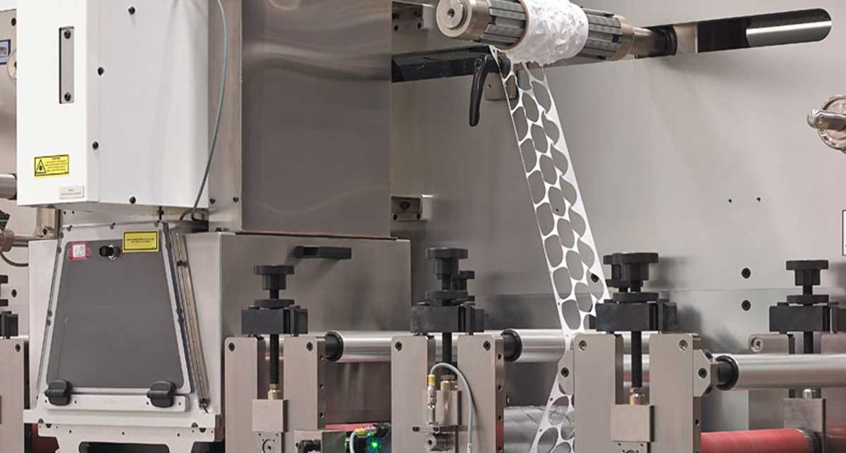
Some solutions, like EMI enclosures, are often heavier, bulkier metal boxes unsuited for transportable devices or lightweight applications. Proper shielding techniques mean choosing the correct material, such as a thin foil instead of a solid metal cage.
In addition, an experienced converter will build your design with the application in mind and create foil tapes in custom lengths, widths, thicknesses, sizes, shapes, and formats based on your needs.
4. USING THE MOST APPLICABLE SHIELDING MATERIAL
The best EMI shielding material depends on many factors, not limited to your product's base materials and function.
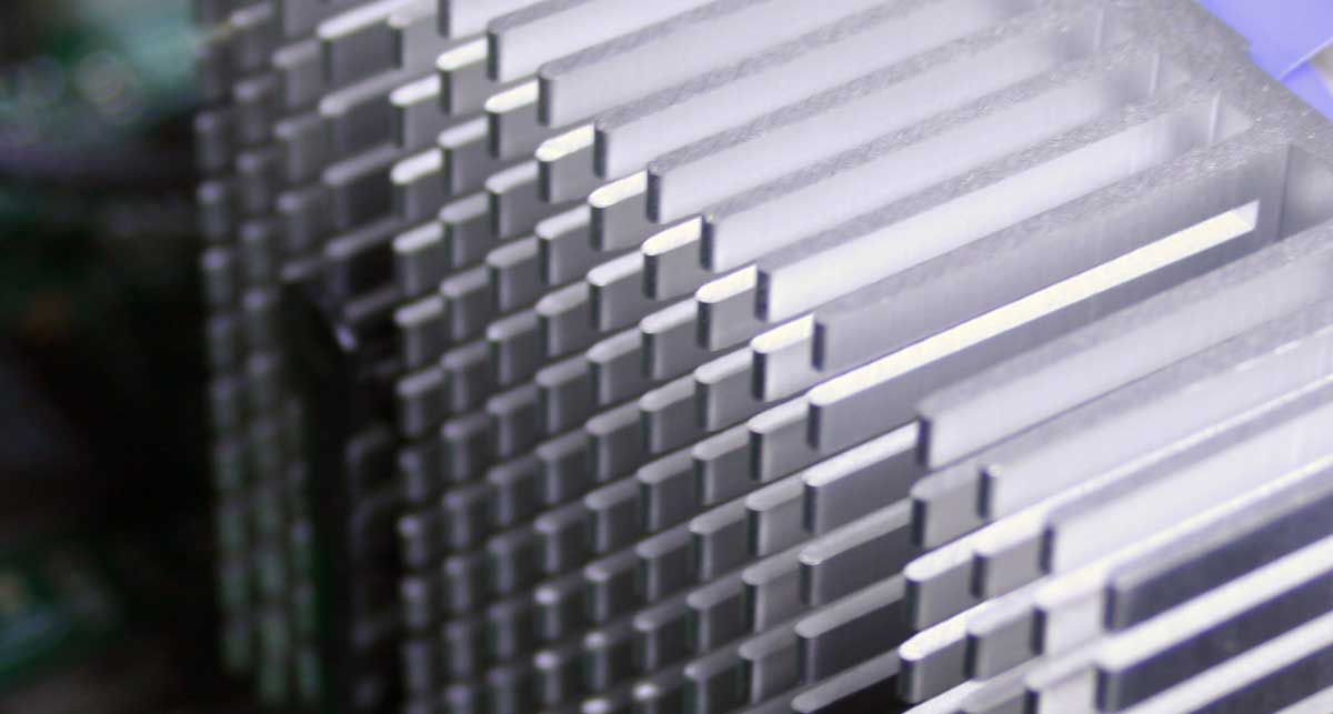
Common EMI shielding materials include plated steel, copper, tin, and aluminum. However, your design’s function will determine the material that works best.
For example, many EMI shielding tapes are built with high conductivity in mind and use conductive adhesive on top of plated foil backings added for electrical interference protection.

Using the wrong material runs the risk of device failure, and it could be challenging to cut and process depending on the device tolerances. Properly sourced materials and the right design and placement will shield EMI and RFI to prevent adverse effects.
Where do you start looking? Get your design evaluated for EMI shielding material recommendations.
5. ADVANCED APPLICATIONS OF SHIELDING SOLUTIONS
Precisely cut EMI and RFI shielding materials can perform shielding functions within tight tolerance devices.
One fast-growing application of shielding technology is within electric vehicles. EV batteries are full of interconnected modules, and the vehicle’s other systems emit signals simultaneously.
With electric vehicle systems such as collision avoidance radars growing in popularity, no one wants to risk the chance of signal interference causing accidents.
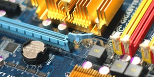
Another advanced solution involves the many shielding precautions added to printed circuit boards. Sensitive technology requires PCBs with built-in, anti-EMI solutions. A “ground plane” protects the system by serving as a PCB EMI shield and by containing any interference from the board.
Lastly, EMI gaskets are commonly used in medical devices to avoid disturbances caused by the other pieces of technology inhabiting the same space.
How Can I Properly Shield Components from EMI?
Shielding your components means placing the right material in the correct position and ensuring proper coverage.
Once you enter production, your converter will send you hundreds, thousands, or even millions of parts. To avoid the possibility of faulty devices, you’ll want to test your material and design before entering into mass production.
You could even test sample parts within the device so you know you’ve successfully dealt with the interference.

Interference is a real cause for concern when designing consumer electronics.
To know more about EMI and RFI shielding solutions, check out the information above or see more applications in our Learning Center.
Originally published: May 10, 2016
.jpeg?width=290&name=0%20(1).jpeg)